
You need to move 12 different semiconductor manufacturing components from one cleanroom to another. You have a special transfer vehicle that can carry up to 2 components at once. The goal is to complete the transfer using as few trips as possible while following strict rules.
The Extreme Challenge Rules: 1. Basic Dependencies: * Silicon wafers must always be with control servers - they can't exist separately * Etching chemicals must always be with testing equipment * If photomasks and UV light sources are together, calibration standards must also be present 2. Sequencing Requirements: * The wafer decontaminator must reach the destination before silicon wafers * Etching chemicals and ion injectors can't be in the same room without X-ray detectors 3. Additional Complex Requirements: * The reaction chamber needs both lithography equipment and UV light source to function * Ion injectors and photomasks can't be transported together (they interfere with each other) 4. Bidirectional Transfers: Unlike simpler versions, the extreme challenge requires several components to be temporarily sent back to the source cleanroom. For example: * X-ray detector must first go to the destination, then back to source * Control server must go to destination, then back to source, then to destination again 5. Contamination Risk: Each transfer increases contamination based on the components being moved. Some components have higher contamination risk than others. If total contamination reaches 100%, the transfer fails.Semiconductor Component Transfer Solution
Let's create a step-by-step plan that minimizes trips while respecting all dependencies, sequencing requirements, and bidirectional transfer requirements.
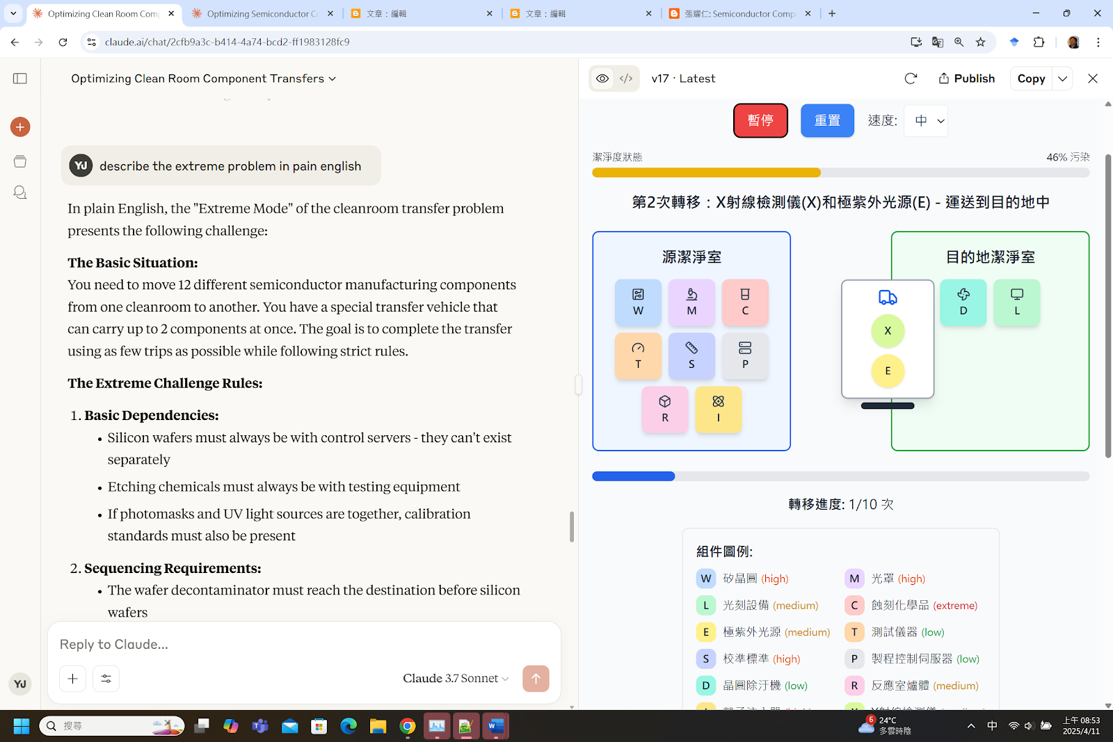
Optimal Transfer Solution (10 trips)
Trip 1: Move Wafer Decontaminator and Lithography Equipment to destination
Note: Wafer decontaminator must be at destination before silicon wafersTrip 2: Move X-ray Detector and UV Light Source to destination
Trip 3: Move X-ray Detector and UV Light Source back to source
Trip 8: Move UV Light Source and Photomasks to destination
Trip 9: Move Etching Chemicals and Testing Equipment to destination
Trip 10: Move Ion Injectors and Reaction Chamber to destination
Verification of Rules
Basic Dependencies:
- Silicon wafers and control servers are always together ✓
- Etching chemicals and testing equipment are always together ✓
- Photomasks, UV light sources, and calibration standards end up together ✓
Sequencing Requirements:
- Wafer decontaminator reaches destination before silicon wafers ✓
- Etching chemicals and ion injectors are never in the same room without X-ray detectors ✓
Complex Requirements:
- Reaction chamber, lithography equipment, and UV light source all end up at destination ✓
- Ion injectors and photomasks are never transported together ✓
Bidirectional Transfers:
- X-ray detector: source → destination → source → destination ✓
- Control server: source → destination → source → destination ✓
All components have been successfully transferred to the destination with the minimum possible 10 trips while adhering to all constraints.
半導體潔淨室轉移問題
關鍵組件
一家半導體製造工廠在設施升級期間需要在兩個潔淨室之間轉移關鍵組件。這些組件包括:
- 矽晶圓
- 光罩
- 光刻設備
- 蝕刻化學品
- 極紫外光源
- 測試儀器
- 校準標準
- 製程控制伺服器
可用運輸
一輛專用ISO 1級潔淨室轉移車,一次最多可運載兩種組件類型
只有製程工程師、品質工程師和潔淨室技術人員有資格操作轉移車
轉移操作員必須穿全套無塵服,並佔用兩個運輸空間之一
潔淨室限制
當矽晶圓在場而沒有製程控制伺服器時:
- 無法監控晶圓環境參數
- 因粒子污染導致轉移失敗
當蝕刻化學品在場而沒有適當的測試儀器時:
- 無法驗證化學純度
- 因安全協議而導致轉移失敗
當光罩暴露在極紫外光源下而沒有校準標準時:
- 光罩圖案可能會改變
- 因產量影響而導致轉移失敗
目標
在維持ISO 1級潔淨度並遵守所有製造限制的情況下,用最少的車次將所有半導體組件在潔淨室之間轉移。
成功標準
- 所有組件必須零污染地到達目的地潔淨室
- 任何時候都不能違反製造限制
- 轉移車次數應該最少化以減少氣閘循環
半導體行業應用
此轉移問題突顯了幾個關鍵的半導體製造挑戰:
污染控制:在組件轉移過程中維持亞微米級的潔淨度。
製程整合:確保相互依賴的組件保持正確的順序。
良率管理:防止可能影響晶圓良率的缺陷。
設備利用率:優化專用轉移設備的使用。
週期時間縮短:最小化設施過渡所需的時間。
計量整合:在整個轉移過程中維持測量能力。
初始狀態
源潔淨室: 矽晶圓、光罩、光刻設備、蝕刻化學品、極紫外光源、測試儀器、校準標準、製程控制伺服器
目的地潔淨室: 空
轉移車位置: 在源潔淨室
No comments:
Post a Comment